Gates (Not Bill)


I have heard everywhere that Boolean logic is the heart of digital memory and more broadly, digital electronics, and also that emory in computers and other digital devices basically rely on Boolean logic to store, process, and retrieve information.
But how ??, how does 0's and 1's store information , Actually I have no clue and I am on the Journey to find out too
So first we have to understand Logic Gates were it all starts from ..
Logic gates are electronic devices that perform Boolean algebra on one or more binary inputs to produce a single binary output.
Essentially, they make logical decisions. This means by applying different combinations of 0s and 1s to their inputs, logic gates can output results based on predefined rules, which are crucial for performing computational tasks.
Again, how does these gates or know these predefined rules ???
The way logic gates know these predefined rules comes down to their physical design and the properties of the electrical components from which they are built, typically transistors (Ps, we talked about transistors in the previous blog)
The fundamental Logic gates
- AND Gate: "For an AND gate, if both inputs are 1 (true), the output is 1. It’s like saying both conditions must be true for the result to be true. This is useful for operations where multiple conditions must be met."
- OR Gate: "An OR gate, on the other hand, outputs a 1 if at least one input is 1. This gate is used where any one of multiple conditions being true triggers a true result."
- NOT Gate: "A NOT gate, or inverter, flips the input: if you input 0, you get 1, and vice versa. This is critical for toggling states and is widely used in memory circuits to control bits."
So I took my time to implement these gates using transistors and switches to understand the basics. For now, to help visualize these gates, our inputs will be switches, and the outputs will be an LED bulb. This setup makes it easy to see the logic gates at work—flip a switch (input) and watch the LED (output) respond accordingly.
In real-life applications, these 'inputs' can be various forms of digital signals—anything from the binary data processed by a computer's CPU to sensor signals in a smart device. These are not manually operated like our switches but are electrical signals that represent 'on' (1) or 'off' (0). The 'outputs', on the other hand, aren't limited to lighting up an LED. They could be anything from moving data into a computer's memory, controlling power to a motor, or sending a command to start a process in industrial machinery.
Components
- NPN Transistor with a beta (β) of 100.
- LED with a forward voltage drop (Vf) of 2V.
- Resistors for base and load.
- Switches to control the input.
- 5V Power Supply.
Calculating Load resistance (RL): since LED's operate with a forward current of 12-20mA, I will be using a desired current of 15mA to be on the safe side
To calculate the Load Resistor (RL)
V = IR
The voltage across the resistor RL is the
total supply voltage minus the forward voltage of the LED.
Voltage across Rl = 5V - 2V = 3V
Rl = V/I = 3V / 15mA = 200Ω.To calculate the Base Resistor (RB) This resistor controls how much current goes into the transistor, making sure it switches on fully without being overloaded.
Ic == Il
and Ic = β.IB
Ib = Ic / β = 15mA / 50 = 0.3mA
Vrb =Vsupply − Vbe = 5V − 0.7V = 4.3V.
Rb = Vbr / Ib = 4.3V/ 0.3A =14.3.7kΩto push a slightly higher base current, in other to ensure a very solid saturation of the transistor
since all the gates are using the same type and model of transistors, and the base current (IB) required to drive each transistor into saturation is the same across all gates, we will use same resistor value for all the gates
Primary Logic Gates
OR GATE
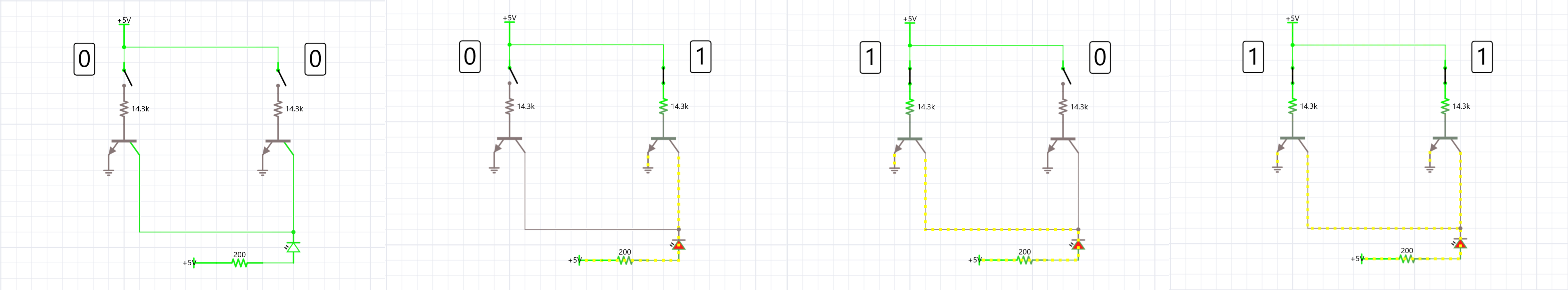
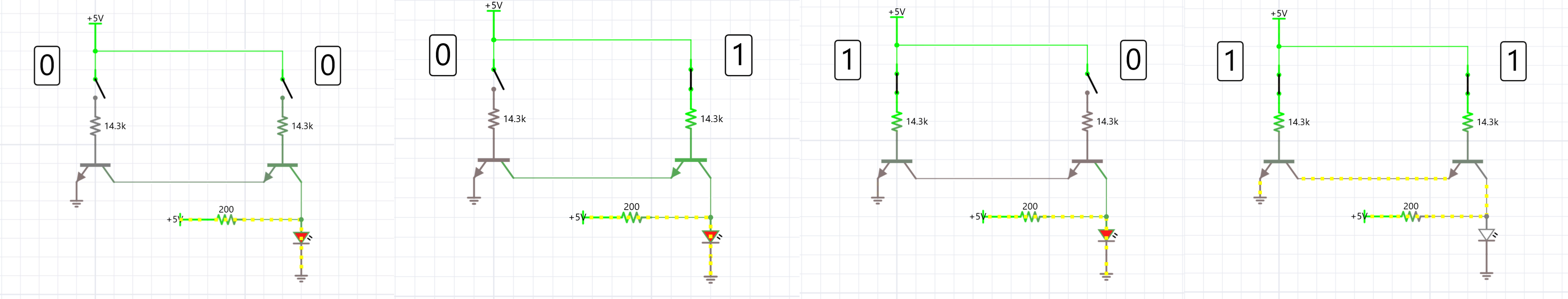
For an OR Gate, 2 NPN transistors are connected in parallel with the load, this means when designing an OR gate using transistors, each input is connected to the base of its own NPN transistor.
The collectors of both transistors are connected together and then to the positive side of the power supply through a load (LED and resistor). The emitters are grounded.
This ensures that if any one of the transistors receives a 'high' (1) signal at its base, it will conduct, allowing current to flow through the load, lighting up the LED — just like if any of the conditions for the OR logic is met, the output is true (1).
AND GATE
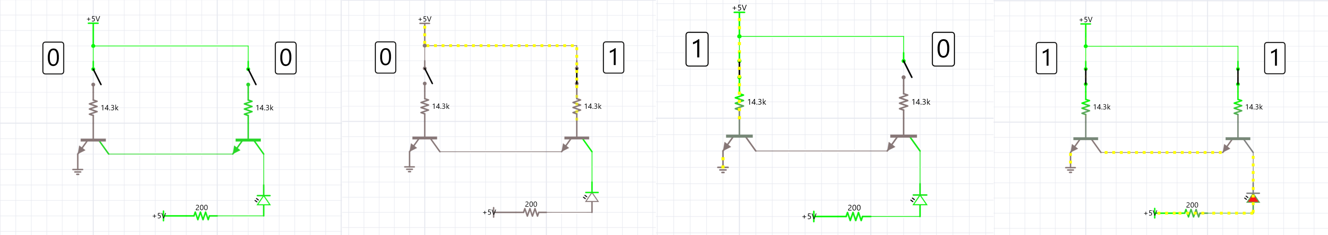
For an AND Gate, 2 NPN transistors are connected in series with the load. Just like the OR, each input is connected to the base of its own NPN transistor.
The emitter of the first transistor is connected to the collector of the second transistor. The collector of the first transistor is connected to the positive side of the power supply, and the emitter of the second transistor is grounded through the load.
With this both transistors must receive a 'high' (1) signal at their bases to conduct, allowing current to flow through the load. Only when both inputs are true (1), reflecting the AND logic, will the LED light up, indicating that the output is true (1).
NOT GATE
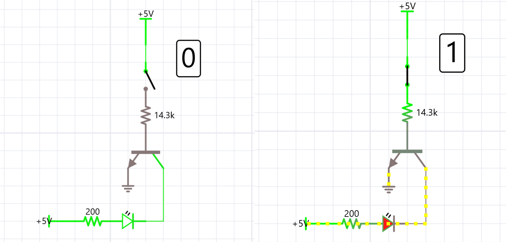
For this, a single NPN transistor is used with the input switch at the base of the transistor as always
The collector of the transistor is connected to the positive side of the power supply through a load, and the emitter is grounded.
Just so when the transistor receives a 'high' (1) signal at its base, it will conduct, grounding the collector and turning off the load. Conversely, when the input is 'low' (0), the transistor does not conduct, and the load remains powered.
the NOT logic, the output is the inverse of the input: if the input is true (1), the output is false (0), and if the input is false (0), the output is true (1).
NOR GATE
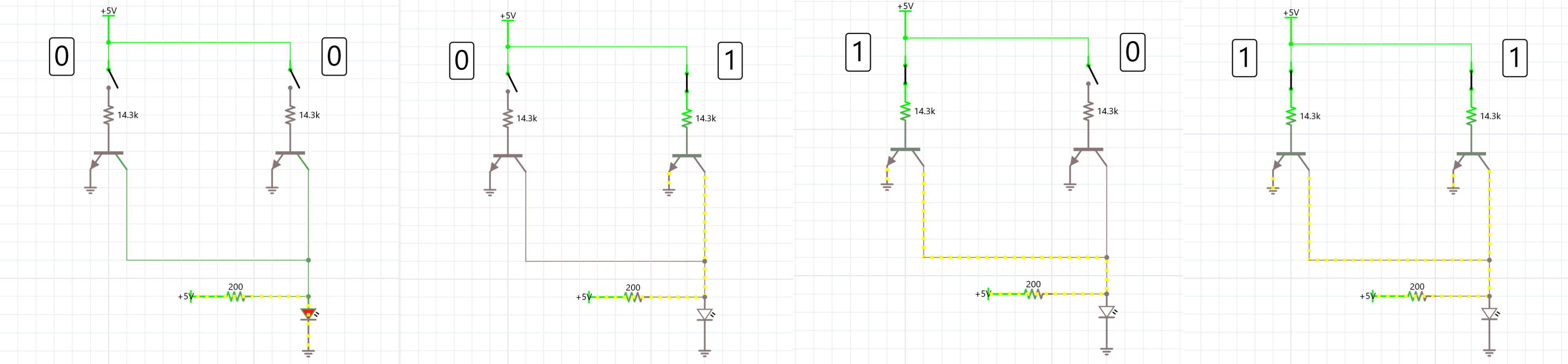 The NOR gate can be thought of as an extension of the AND gate, with an inversion of the output. This means OR + NOT, theoretically it is a combination of OR and NOT, this means we will be connecting the output of the OR to a NOT, so we would use 3 transistors, while this would work perfectly, we can also achieve this with 2 transistors by tweaking the OR gate, by by grounding the load of the OR gate, this inverts the output naturally without the need of a NOT gate
Grounding the load acts as a pull-down mechanism, so as to ensure that the output is normally low when any of the transistors is conducting. When both transistors are off (I.e., both inputs are low), there is no path for the current to complete through to the ground, causing the load to pull the output high.
NAND GATE
Similar to the NOR gate, grounding the load inverts the output. this grounding ensure that the output is high when any of the transistors is conducting. When both transistors are off (I.e., both inputs are low), there is no path for the current to complete through to the ground, causing the load to pull the output high.
I hope this explanation makes sense to you, though it’s perfectly okay if you're feeling a bit confused at this point, I encourage you to research how transistors work Next up, I'm going to attempt to build adders !